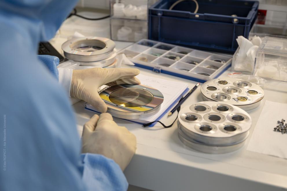
AMUtech 2026 Doctoral Programme – Part 2: Nanofabrication and Nanoengineering
10 November to 14 December 2026 – Saint-Jérôme and Luminy Campuses – Marseille
AIM
The AMUtech Institute is offering the second part of its 2026 doctoral programme, ‘Advanced Materials and Nanotechnologies’, dedicated to nanofabrication and nanoengineering.
This programme aims to familiarise participants with the main methods of developing, manufacturing and integrating nanomaterials and nanotechnological devices. It combines theoretical teaching with practical work on the technological platforms of Aix-Marseille University.
TARGET AUDIENCE
Designed to be interdisciplinary and accessible without any specific prerequisites, the programme is primarily aimed at PhD students in physics, chemistry and engineering sciences wishing to deepen their knowledge and broaden their skills.
It is also open to Master’s students, engineers and researchers with an interest in nanotechnologies.
TARGETED SKILLS
By the end of this course, participants will have gained a better understanding of the main nanofabrication techniques, their potential and their limitations. They will be able to identify the appropriate methods for the fabrication, characterisation and integration of nanostructures into technological devices.
THE COURSES
I. NANOFABRICATION METHODS (11 H)
This first module presents the main methods for fabricating nanomaterials, ranging from bottom-up and top-down approaches to soft chemistry and electrochemical methods. The lectures draw on the techniques and equipment available at Aix-Marseille University’s technology platforms.
I.1 / Bottom-up methods (PVD, CVD, ALD), Luc FAVRE – Tuesday 10 November 2026, 4.00 pm to 6.00 pm: Presentation of the main techniques for depositing thin films at the nanometre scale and their applications, particularly in microelectronics.
I.2 / Top-down methods (lithography, RIE), Igor OZEROV – Thursday 12 November 2026, 2.00 pm to 4.00 pm: Introduction to micro- and nanofabrication techniques in a cleanroom: optical and electronic lithography, etching and deposition, with examples of applications in biophysics, photonics and materials science.
I.3 / Lithography practical session (4 places), Igor OZEROV – Monday 16 November 2026, 9.00 am to 12.00 pm: Practical work in a cleanroom focusing on the stages of microfabrication: deposition of a thin metal layer, lithography, plasma etching and characterisation of the resulting structures.
I.4 / Mild chemistry methods (supramolecular, sol-gel, colloids), Éric BESSON - Wednesday 25 November 2026, from 2.00 pm to 4.00 pm: Presentation of methods for the preparation of materials at low temperatures and the mechanisms for controlling their composition, structure and properties.
I.5 / Electrochemical methods (coating fabrication and nanostructuring), Luca PASQUINI - Thursday 26 November 2026, 2.00 pm to 4.00 pm: An introduction to electrodeposition and electrochemical nanostructuring processes, as well as the parameters used to control the properties of the resulting materials.
II. NANO-ENGINEERING AND INTEGRATION (9 H)
This second module focuses on the optical properties of nano-objects, the integration of functions into devices, and applications of nanophotonics. It also includes practical sessions on nanofabrication and characterisation equipment.
II.1 / Optical spectroscopy at the nanoscale, Jérôme WENGER – Friday 27 November 2026, 2.00 pm to 4.00 pm: An overview of the optical responses of nano-objects (absorption, scattering, fluorescence, Raman, non-linear effects) and their applications in optical detection at the nanometre scale.
II.2 / Integration of functions into devices, Rémi VAUCHE - Wednesday 2 December 2026, from 2.00 pm to 4.00 pm: Presentation of the stages involved in the integration of electronic functions, from microelectronic processes to advanced packaging and 3D assembly techniques.
II.3 / Plasmonics and optical chirality: towards light-controlled asymmetric photocatalysis, Artur MOVSESYAN - Monday 7 December 2026, 2.00 pm to 4.00 pm: An introduction to plasmonics, optical chirality and their applications for controlling light-matter interactions and photochemical reactions.
II.4 / Practical session: Electron lithography or FIB-SEM microscopy ( 3 places), Frédéric BEDU – Monday 14 December 2026, 9.00 am to 12.00 pm: Practical sessions offering an introduction to advanced techniques. Electron lithography: creation of nanometre-scale patterns using a focused electron beam, from sample preparation to characterisation. OR FIB-SEM Microscopy: an introduction to the principles and applications of the focused ion beam for the preparation, modification and characterisation of materials at the nanometre scale.
Course venue: Room 1 Étoile Nord, Saint-Jérôme campus, Marseille, with the exception of the practical sessions, which will be held at the PLANETE facility in Luminy.


